
PZT Electrode Design Before Wiring: Layouts, Gaps and RFQ Checklist
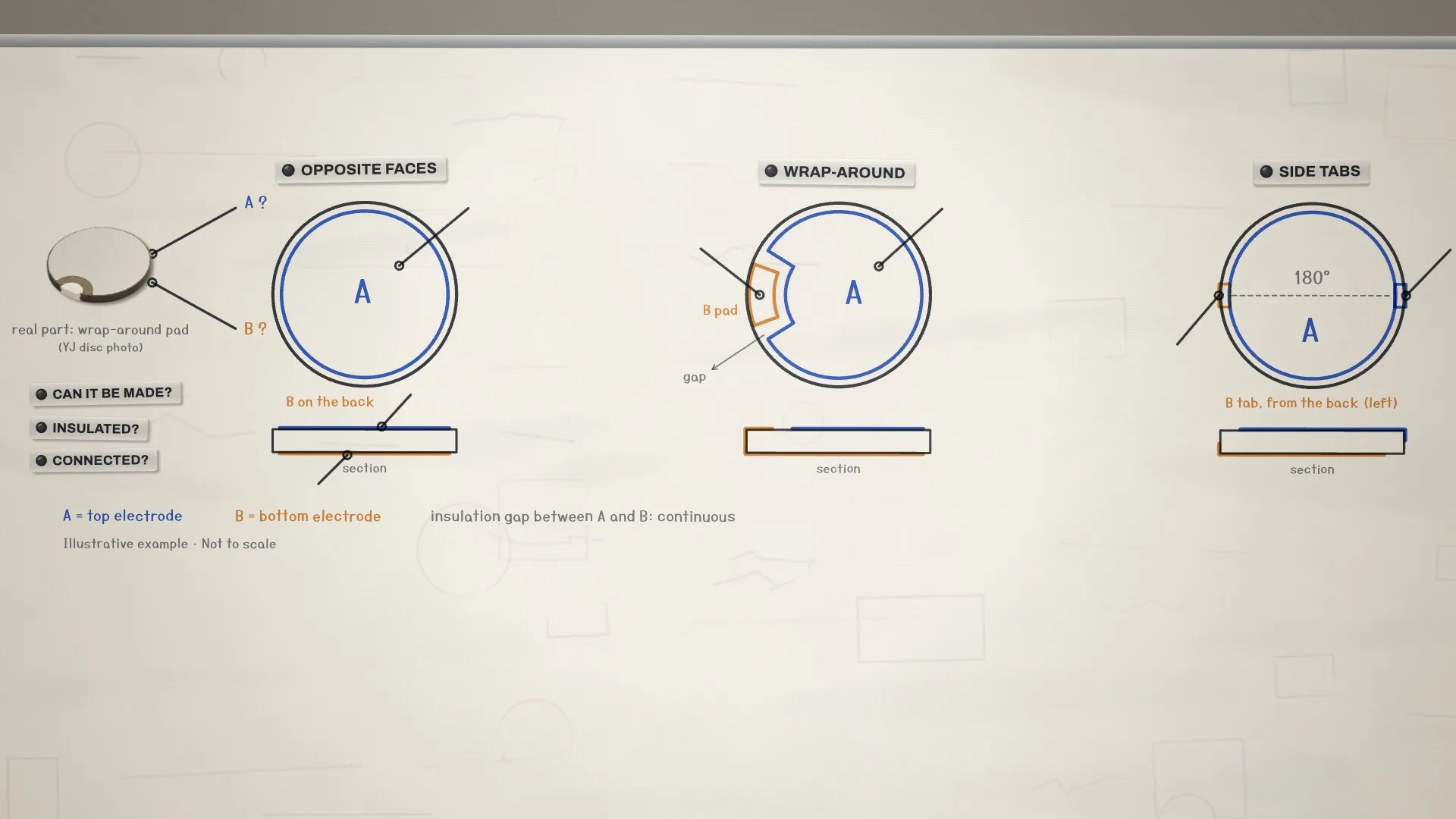
Before attaching wires to a PZT ceramic, identify both electrodes, trace their complete paths and confirm the connection areas and insulating gaps. Two accessible soldering points do not establish that a pattern is manufacturable or suitable for your assembly. This guide is for OEM engineers and buyers preparing a custom part, a replacement or a sample evaluation.
Start with the geometry and mounting constraints you already know. If both connections must be accessible from one side, explain why. That requirement may change electrode coverage and the manufacturing review. An initial discussion can begin with a sketch and clearly marked open questions.
Video: check the electrode layout before wiring
This 4-minute YJ Piezo video compares three layouts and two generic design problems. English narration and English captions are available on YouTube. The examples are redrawn for teaching and contain no customer documents or test results.
Watch the electrode design video on YouTube.
Distinguish three electrode layouts
Use front, back and side views to identify electrode A and electrode B. Keep those identities separate from the poling-direction arrow. The names below describe connection arrangements, not a guarantee that each pattern is available for every geometry.
| Layout | Connection path | What the drawing must show |
|---|---|---|
| Opposite-face electrodes | A is on one broad face and B is on the opposite face, with one connection on each. | Identify both faces, connection zones and the wire access required after mounting. |
| Single wrap-around return | One electrode returns around an edge to an isolated pad on the other face, allowing both connections from that face. | Show the return path and a continuous insulating separation around the returned pad. Review the remaining main-electrode area. |
| Separate side tabs | The two face electrodes extend to separate areas on the side surface. | Show which tab belongs to which face and every local gap to the other electrode. Tab positions alone do not define the separation. |
APC International describes wrap-around and side-tab patterns as different arrangements. Its published manufacturing rules apply to its own products. Use the distinctions to clarify your drawing, then ask YJ Piezo to review the actual part rather than copying another supplier's dimensions as a YJ specification.
Two teaching examples: when an accessible pad is not enough
Both examples below are hypothetical and have no production dimensions, customer identity or claimed performance result.
Example 1: a thick plate with a wrap-around pad
Suppose a housing makes one-face access convenient, so a thick plate is drawn with a return pad. The insulating band needed for that layout may occupy a significant part of the available electrode surface. The useful question is not simply whether metal can be printed around the edge: can the pattern be made while retaining electrode coverage suitable for the application?
Ask the supplier to review thickness, return-pad size, insulating separation and remaining coverage together. A wrap-around layout may be possible yet unattractive for the design. If the assembly allows access to both faces, compare opposite-face connections and validate the revised part in the actual mounting. Do not assume a universal thickness cutoff or a fixed percentage loss in performance.
Example 2: a small disc with two side tabs
Suppose two tabs are placed on opposite sides of a disc. A 180-degree position difference does not tell you the nearest distance between each tab and the other face electrode. Trace A and B through the side view and mark both local gaps. Inadequate separation can create a risk of electrical breakdown during poling.
If the required gaps cannot be maintained, revise the electrode pattern. Opposite-face connections are one possible alternative if the customer can accommodate the changed assembly. Confirm the new drawing and sample checks before treating the alternative as interchangeable.
Separate poling risk from connection-process risk
Poling breakdown concerns the electrode geometry and the manufacturing electric-field process. Soldering introduces a different question: whether the electrode and ceramic can tolerate the joining process. CTS notes that prolonged solder contact can dissolve screen-printed silver and that heat transfer can risk depolarization. A part-specific joining window is needed; its published temperatures and times are not YJ Piezo process limits.
Review soldering, conductive adhesive or supplied leads against the actual metallization and part. Confirm who supplies the connection, the allowed contact area, process exposure, rework conditions and inspection scope. For adhesive joining, select the material and cure conditions for the specific assembly. Route and secure wires so external handling does not pull directly on the electrode joint.
Agree what the sample review will check
- Geometry: electrode identity, continuous separation, pad position, wire exit and mounting clearance against the agreed drawing revision.
- Insulation: the method, applied conditions, acceptance limits and sampling agreed for the actual component. This article provides no universal gap or test-voltage prescription.
- Electrical and piezoelectric behavior: relevant measurements before and after connection using comparable fixture and measurement conditions, followed by evaluation in the intended assembly.
What to send for an electrode-layout review
Use this checklist with your drawing. Mark a value as unknown when it is still open rather than filling it with an unrelated catalog number.
- Part shape, dimensions, units, tolerances that matter, and drawing revision.
- Front, back and side views showing A/B electrode paths, poling direction if known, connection zones and the gaps to be reviewed.
- Why the connection location is constrained, including mounting, bonding, housing access and wire routing.
- Known material or performance priorities, drive or signal conditions, duty cycle, temperature and operating medium.
- Whether you need bare ceramic or a connection/assembly review, plus sample quantity and expected purchasing quantity.
- Validation goals, requested inspection records, fixed requirements and open questions.
Need a custom PZT electrode layout? Send YJ Piezo your drawing, electrode pattern, connection locations, known operating conditions and sample quantity. Mark any open questions so we can review manufacturability and the sample plan with you.
Request a custom piezoelectric component review.
For the broader enquiry, use the PZT ceramic RFQ template. For material, geometry and integration choices, continue with the custom PZT component guide.
Technical sources and scope
Manufacturer references support general design and joining considerations. They do not establish YJ Piezo tolerances, minimum order quantities, lead times, certifications or results for your part. Feasibility and supply scope are confirmed after review.